Some background - the Metcal irons use RF to heat the tip, there are two systems, both in ISM bands. This method of heating allows very good thermal contact between the heater and the tip. It also allows the temperature to be very precisely controlled by the choice of materials in the tip - it gets regulated pretty tightly to the Curie temperature of the material used. For the user this means that they heat up fast, maintain their temperature well, and even small tips can deliver a lot of heat to a large ground plane or similar. There's a good description of the technology here. The newer system works at 13.56 MHz and that's what I have built.
This Metcal power supply is based on, and uses PCBs from, a design by mamalala, see the long thread on eevblog. I have made a few changes and additions, these are described below. Thanks also to zayance for ordering another batch of the PCBs and selling them to me at cost.
Most images on this page are low resolution versions. Click them for bigger versions.
Design description
Read the long forum thread for the full details but essentially it's a single MOSFET RF amplifier using an IRF510 driven at 13.56 MHz from a small crystal oscillator. A switching power supply provides power to the drain load of the MOSFET and regulates for constant RF voltage at a point in the output filter which approximately corresponds to constant RF current through the load. Into a nicely matched 50 Ohm load it can deliver 50 Watts or so. When the tip reaches temperature it reflects more power, the voltage on that filter node rises, the power supply winds back and the power delivered to the load falls dramatically.
So far as I can tell there are no matching components in the hand-piece, it it looks a bit capacitive when un-terminated and measures about an Ohm end-to end. It's possible there might be a series L and/or shunt C but I suspect there isn't and I'm just seeing the cable. At d.c. the tip itself looks like a dead short as expected.
| Measurements at 13.56 MHz of a STTC-147 tip | |||||
|---|---|---|---|---|---|
| R | X | Equiv X | SWR | S11 | |
| Cold: | 42.3 | +13j | 153 nH | 1.4 | -16dB |
| Warm (but below Curie temp): | 55 | -16j | 730pF | 1.1 | -23 dB |
| Hot (above Curie temp): | 12 | +24j | 280 nH | 5.1 | -3.4 dB |
There's a gradual sweep from cold to warm that passes through a near perfect 50 Ohms, then there's a quick transition at the Curie temperature to a low impedance with a lot of inductance. Notice that even at this point return loss is still better than -3dB - more than half the power is absorbed, this is the reason for the current source drive - constant voltage drive from 50 Ohms would only give a 50% reduction in power when hot, not enough.
The design also includes a power measurement circuit, a microcontroller and a 16x2 character LCD. This is not required for the main functionality but it allows fun features such as realtime power measurement and auto sleep modes. The auto sleep is very nice, the software looks for changes in power and if none are seen it assumes the iron is sat idle in its stand and goes to a reduced power mode. Crucially it's still a bit warm, enough that picking up the iron and waving it through the air produces a detectable change in power and kicks it from “sleep mode” into “boost mode” which rapidly warms it up for soldering - the user doesn't even notice it went to sleep but still gets the tip life improvements.
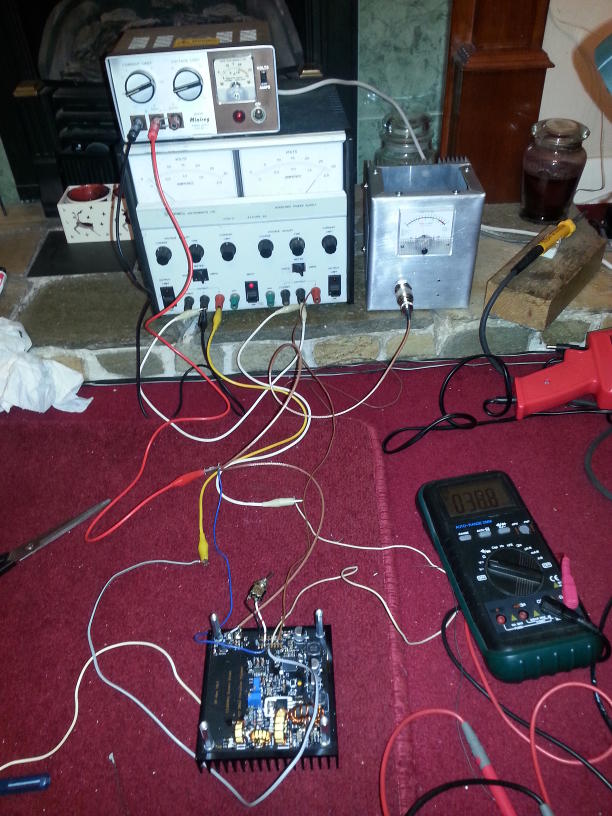
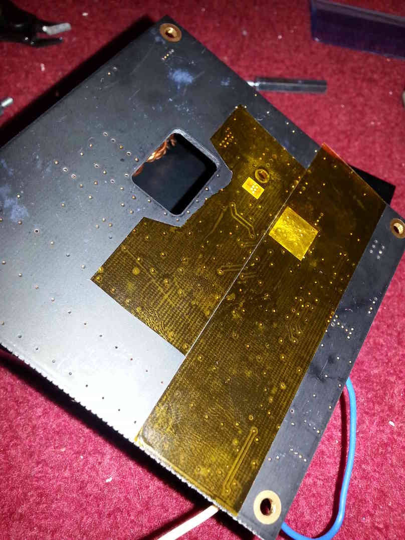
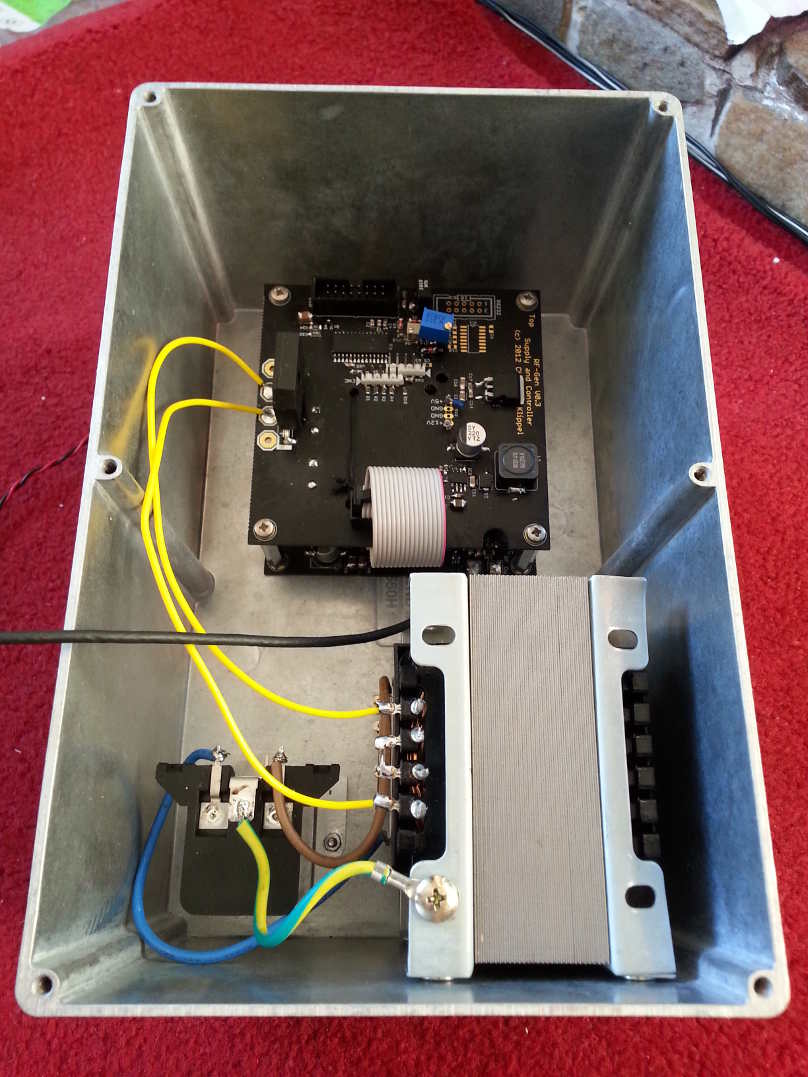
The electronics is split across two PCBs. The RF board takes DC in at about 30V and generates a variable supply for the MOSFET drain and the gate drive signal. It contains the RF output filters which include a number of hand-wound components. It has a few op-amps providing the feedback for the drain main switching supply and also buffering signals used on the other board. The seemingly blank area of the PCB actually contains a printed directional coupler used to give the microcontroller a measure of forward and reflected power. The RF board works standalone and may be used to power a soldering iron without the control PCB.
The control PCB contains a PIC18F microcontroller, various power supply related parts that provide 30V, 12V and 5V to the control board and an RS232 level shifter that I chose not to fit. It sits directly above the RF board connecting via a 16 pin ribbon. Another such ribbon connects to the 16x2 character display. This board provides all the additional functionality such as smart sleep functions.
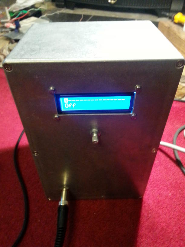
Boxing it up
Kapton tape was applied to the rear of the PCB to provide insulation where there are tracks on the bottom layer. The PCB has a rectangular hole for the TO-220 output transistor, a corresponding hole was cut into the enclosure. The heatsink was prepared with tapped holes in the corners and on the transistor location. The PCB mounts directly onto the inside of the enclosure with heatsink grease, this provides heatsinking for the board itself, particularly the areas under the switcher and the gate driver IC (these are the regions with no black soldermask and lots of vias). The output transistor passes through the hole in the case and is mounted on the heatsink with a mica washer and more thermal grease. Thermal grease is also used between the case and the heatsink for better contact between these. The intention is for the whole assembly to be a single thermal mass.
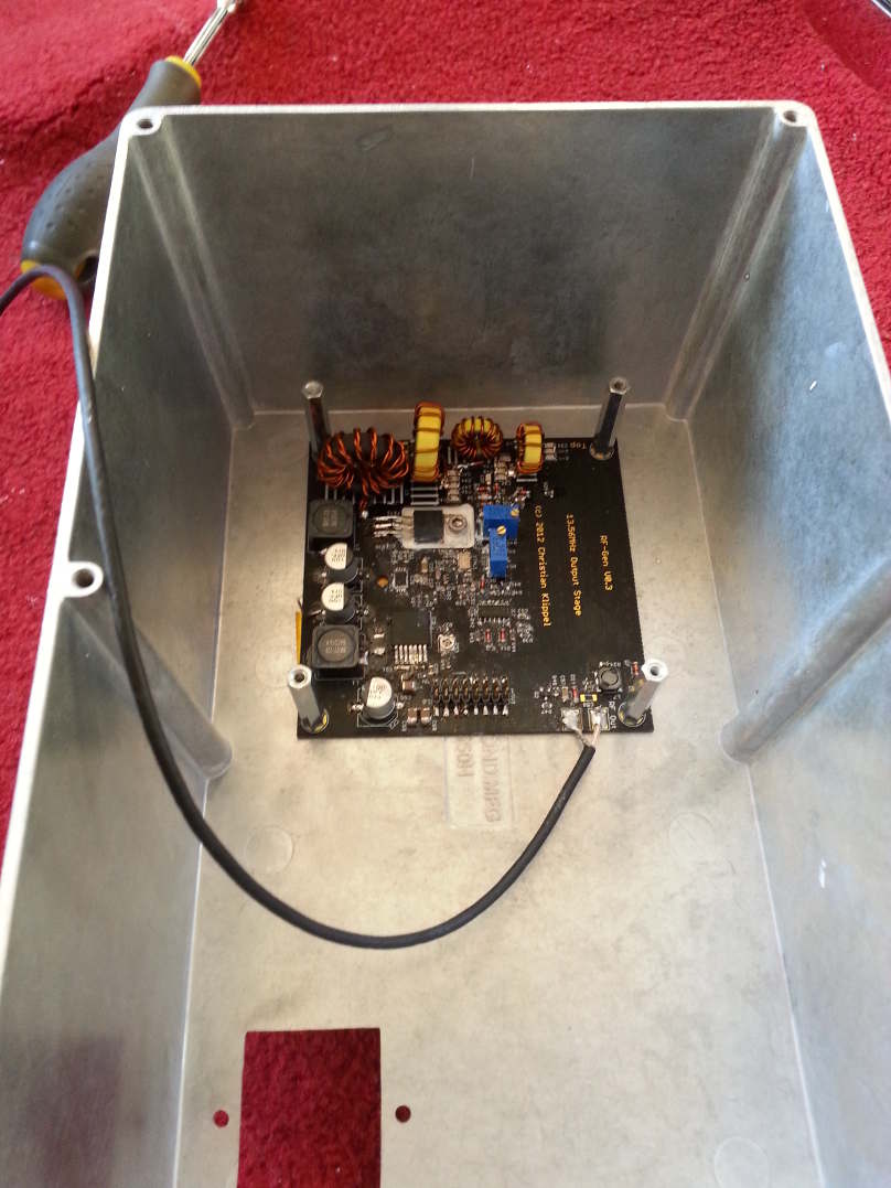
The long threaded pillars pass through both PCB and case and into the tapped holes in the heatsink, holding the whole assembly together. These then provide the support for the control PCB which sits i the same footprint. The threaded pillars are an unusually long length ordered specially to allow the large electrolytics on the control PCB to be mounted underneath. The mains transformer and a filtered IEC inlet with built-in fuseholder were mounted in the bottom of the case.
Undervoltage lockout
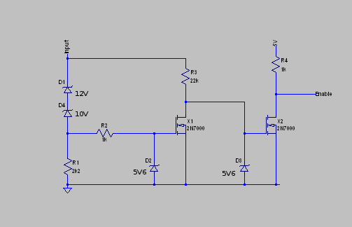
A known bug of the design is that, very rarely, if the power supply is removed whilst the RF is on the buck converter or the RF output FET can be damaged. To work around this an undervoltage lockout circuit was added to the board. This disables (using the same line as tip detect) the supply if the input voltage drops below around 22 Volts.
DC input
I've built the supply with a conventional 50 Hz transformer for the mains input but added an additional power input based around a cheap Ebay boost converter module. It's rated for up to 10 A output at between 10 and 60V. I modified it to use the enclosure as it's heatsink and to output a fixed 33V. It also has an adjustable input current limit which I have set to allow for full power at the lowest expected input voltage of 10V.
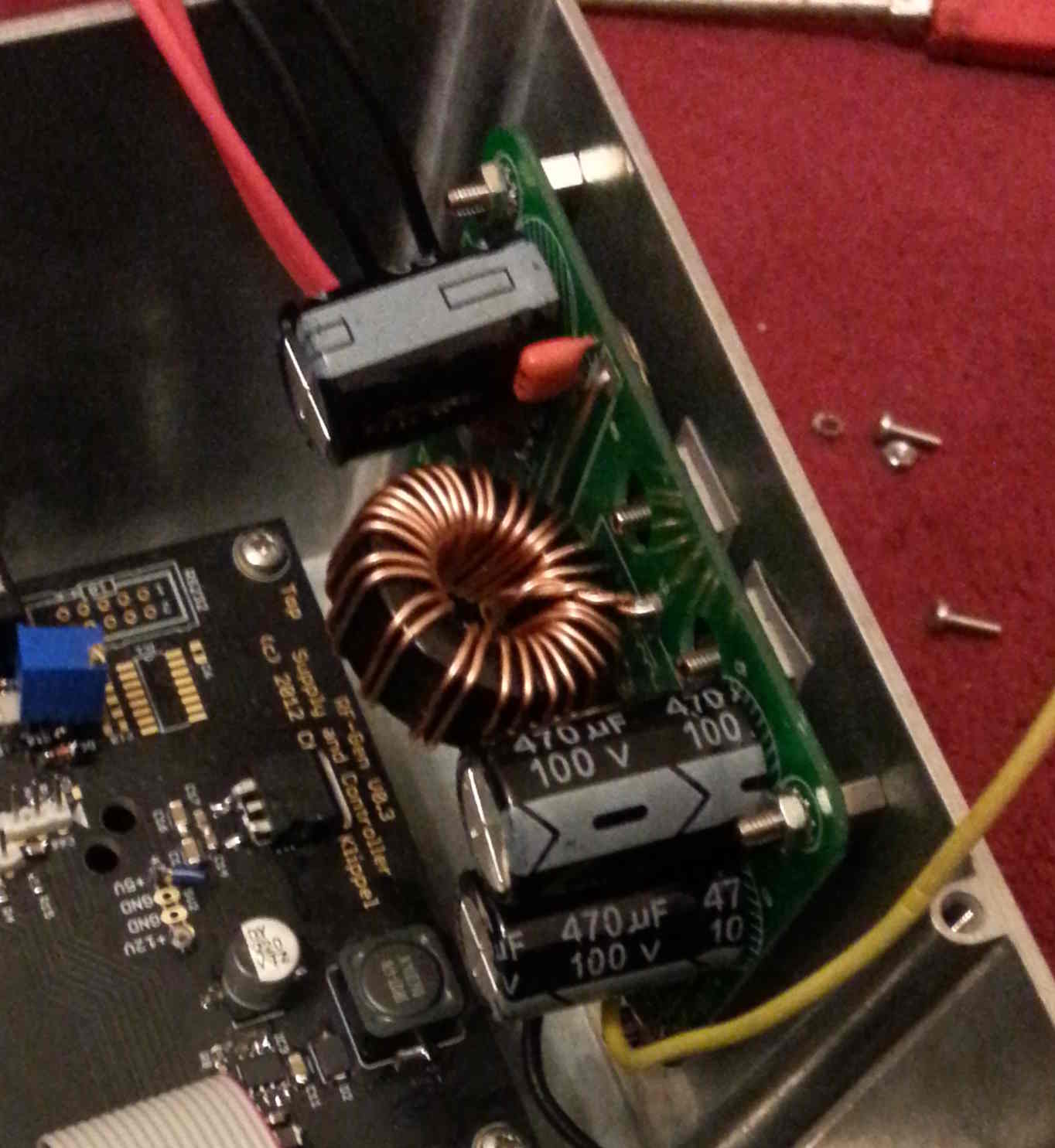
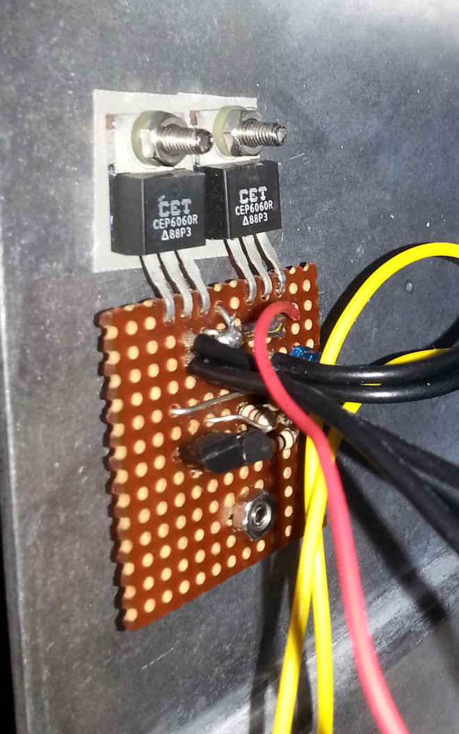
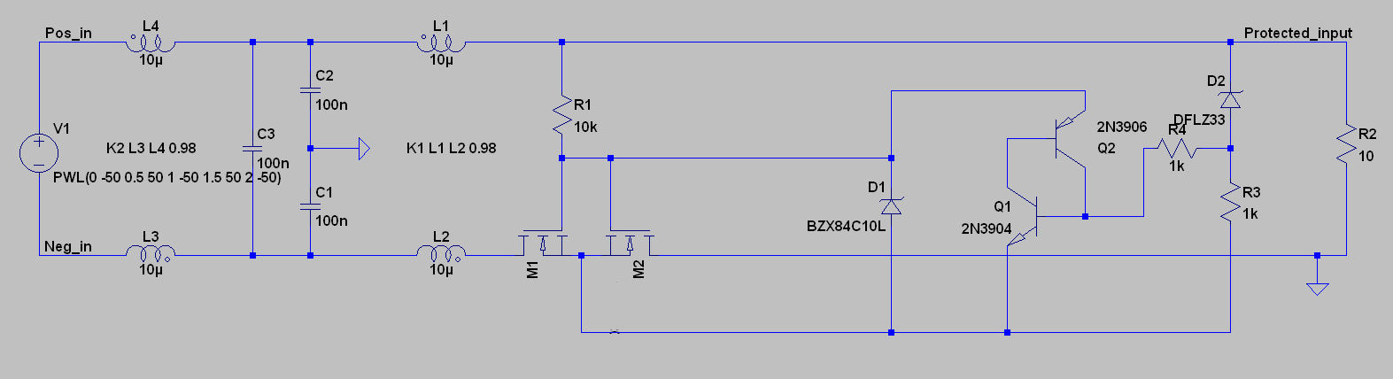
I also added an overvoltage and reverse polarity protection circuit. This uses source-to-source N-channel MOSFETs to isolate the negative input in the event of reversed polarity or if the input exceeds about 32 Volts. This allows powering from a 28V d.c. supply but prevents damage to the downstream circuitry if higher voltages were to be connected - the boost converter would simply pass these through with only a single diode drop. Click here for the schematic of the input protection and filtering. Note that the input filtering shown on the schematic is fitted to the back of the DC input connector not to the small board with the MOSFETs.